The complete guide to PCB pad :types, size, spacing, repair and
Soldering is one of the most important processes in PCBA processing. On printed circuit boards, electrical connections to all components are made via PCB pads. The PCB pads are a very critical part of the PCB that determines where components are soldered on the PCB.The size, shape, and position of pads in a PCB directly depend on the manufacturing quality of the board. Today we will take a look at the PCB pad in SMT soldering.
Soldering is one of the most important processes in PCBA processing. On printed circuit boards, electrical connections to all components are made via PCB pad.
The complete guide to PCB pad :types, size, spacing, repair and comparison - IBE Electronics

PCB Pad Size Guidelines: Finding the Proper Pad Sizes for Your Circuit Design

What is reflow soldering? Technological process, defects and comparison with wave soldering - IBE Electronics

LG Innotek launched the world's thinnest semiconductor package substrate - IBE Electronics

How to solve the solder scooped on welding? - IBE Electronics
How to Troubleshoot and Repair Your PCB
PCB Layout: A Comprehensive Guide

PCB Etching : a guide to materials, methods, and safety precautions - IBE Electronics
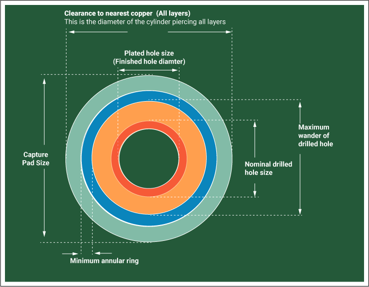
What is a Pad in PCB Design and Development