pcb - What is the pad size required for this BGA AW H3 Chip
I'm trying to figure out the pad size to use for my footprint according to this datasheet.The last page in the datasheet has the package dimensions. I've also posted the relevant information in a p

PCB Pads shape and size design standards
PCB Basic Knowledge_37

pcb design - Unknown indicator of package specification - Electrical Engineering Stack Exchange

Why does the underside of this flip-chip BGA have small notches in it? - Electrical Engineering Stack Exchange

Repair damaged BGA chip pad
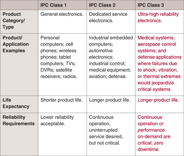
Clash Between IPC Class 3 Requirements & Shrinking Geometries

Which BGA Pad and Fanout Strategy is Right for Your PCB?
pcb - Solder Mask Expansion Rules and Passive design in Altium - Electrical Engineering Stack Exchange
BGA Design Guidelines - PCB Layout Recommendations for BGA packages
Technical Guidance: BGA Design Rules

BGA Pad Size Deep Dive Component Creation